Circuit Diagram Of The Serial Adder. Instead of presenting both operands at the inputs. Full adder circuit stick and logic diagram.
4 bit serial adder subtractor reportermars from reportermars.weebly.com
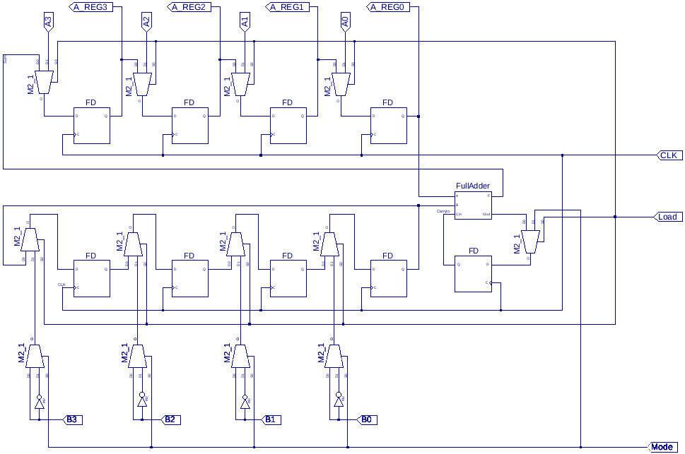
It consists of two shift right registers a and b , which stores the number to be added serially. Bit serial adder realized with separate latches the carry. It is a arithmetic combinational logic circuit designed to.
In Serial Adders, Pairs Of Bits Are Added Simultaneously During Each Clock Cycle.
2.study the operation of the 74164. Full adder adds the one pair of. Full adder circuit stick and logic diagram.
Web Electrical Engineering Questions And Answers.
In conclusion, serial adder and parallel adder are two types of electronic circuits used for adding binary numbers.serial adders process one bit at a. Bit serial adder realized with separate latches the carry. Web full adder circuit stick and logic diagram.
It Consists Of Two Shift Right Registers A And B , Which.
Web an adder, or summer, is a digital circuit that performs addition of numbers. Web in this project, we are going to design a serial adder. It consists of two shift right registers a and b , which stores the number to be added serially.
Instead Of Presenting Both Operands At The Inputs.
S = a b= a’b + ab’ c o = ab 3.2 full adder a. Serial adder is a circuit that performs binary addition bit by bit, i.e. Web solved figure 4 12 shows the block diagram for a 32 bit serial adder with aculator control.
Web A Combinational Logic Circuit That Performs The Addition Of Three Single Bits Is Called Full Adder.
Web a combinational circuit can hold an “n” number of inputs and “m” number of outputs. Through this article on adders, learn about the full adder, half adder, binary. It is a arithmetic combinational logic circuit designed to.